我组关于'调整相结中的内置电场来促进光催化水分解'的文章被J.Mater.Chem.A期刊接收!同时被选为当期封底文章
日期:2019.07.15
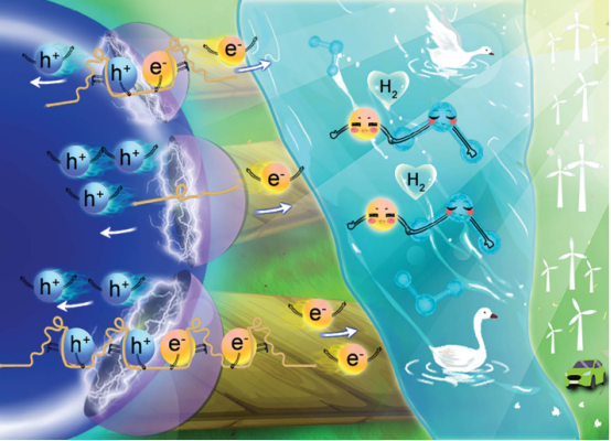
Title: Boosting photocatalytic water splitting by tuning built-in electric field at phase junction
DOI: 10.1039/C8TA08199A
Website: https://pubs.rsc.org/en/content/articlelanding/2019/ta/c8ta08199a#!divAbstract
Abstract: Constructing a built-in electric field at the interface of semiconductors has been demonstrated to provide the driving force for spatial charge separation in photocatalysis. Although phase junctions (interfaces formed between two crystalline phases of the same semiconductor) have been demonstrated to be effective in spatial charge separation, regulation of the photocatalytic activity by precisely tuning the built-in electric fields is not yet well understood. In this work, taking anatase/rutile TiO2 phase junction as an example, the built-in electric field in the phase junction region was modulated via fabricating controllable anatase nanoparticles on rutile TiO2 surface to manipulate the interfacial contact area between anatase and rutile phases. We found that photocatalytic H2 evolution depends strongly on the interfacial contact area between anatase and rutile TiO2. The relation between the anatase/rutile phase junction interfacial contact area and the specific photocatalytic activity shows a typical volcano curve, that is, increasing the interfacial contact area results in enhancement of the driving force for spatial charge separation, allowing more electrons and holes to migrate to the surface and participate in redox reactions, but further increasing the interfacial contact area leads to decline of photocatalytic activity. The optimized interfacial contact is the most favorable balance between the strength of built-in electric field and transfer distance for photogenerated charge carriers for separation and transfer of photo-generated electrons and holes at the phase junction region. Our work provides new insight into the construction of built-in electric fields on the surface of semiconductor-based photocatalysts to boost spatial charge separation for solar energy conversion systems.
光催化中半导体形成的“结”结构可以在其接触界面处形成一个内建电场,为空间电荷的分离提供驱动力。同一半导体的两种不同晶相间形成的“异相结”,能够提供能带弯曲的连续性,从而有效地加速跨界面电荷的转移,成为光催化中实现光生电荷分离的有效策略之一。那么,如何通过精确调节“异相结”的内建电场来调节空间电荷的分离,进而调节催化剂的光催化活性?针对此问题,考虑到“异相结”的内建电场与两相界面接触面积密切相关,我们通过控制“异相结”表面晶相粒子大小来调变两相界面接触面积。我们发现,合适的界面接触面积可以优化内建电场的强度和作用范围,驱动电子和空穴的分离与迁移,从而增强光催化活性。上述工作为半导体光催化剂内建电场的构建提供了新的见解,对有目的的设计和开发出更高效的具有“结”结构的半导体光催化剂具有理论指导意义。